

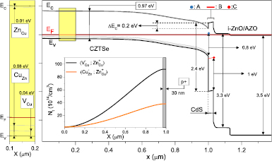
Modelling of Cu2ZnSnSe4-CdS-ZnO thin film solar cell
We present a device model for the Cu2ZnSnSe4-CdS-ZnO solar cell with a total area efficiency of 9.7% reported in 2013 (Brammertz et al 2013 Appl. Phys. Lett. 103 163904). The simulations were performed using SCAPS program. In the device model, we reproduce rigorously the full range of layers and device properties estimated experientially using various characterization techniques. We include in the device model barriers at the back contact and the absorber/buffer interfaces, the photo-doped CdS buffer layer and defect states at the CdS/ZnO interface. A perfect match with the electrical behaviors of the solar cell are obtained, including light and dark current voltage, quantum efficiency, open circuit voltage (V OC) versus temperature and capacitance measurements. We show as well that interface recombination does not have an impact on the V OC deficit but partially reduces the short circuit current and the fill factor and that the main electrical limitations are due to the presence of tail states and electrostatic potential fluctuations in the CZTSe material leading to a decrease in the band gap and an increase of radiative recombination by tow orders. © 2017 IOP Publishing Ltd.