
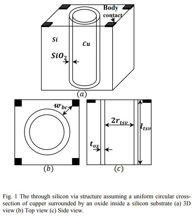
Compact lumped element model for TSV in 3D-ICs
A wide-band lumped element model for a through silicon via (TSV) is proposed based on electromagnetic simulations. Closed form expressions for the TSV parasitics based on the dimensional analysis method are introduced. The proposed model enables direct extraction of the TSV resistance, self-inductance, oxide capacitance, and parasitic elements due to the finite substrate resistivity. The model's compactness and compatibility with SPICE simulations allows the fast investigation of a TSV impact on a 3-D circuit performance. The parameters' values of the proposed TSV model are fitted to the simulated S-parameters up to 10 GHz with an error less than 5%. It is shown that a TSV capacitance is highly dependent on the positions of ground contacts and has a value of tens of femto farads in a typical current technology. This value is much higher than a minimum device capacitance and requires special design methodologies such as cascaded buffers. Coupling between TSVs will be handled in another paper. © 2011 IEEE.
Related Publications
Hands-on analysis of using large language models for the auto evaluation of programming assignments