
3D/TSV enabling technologies for SoC/NoC: Modeling and design challenges
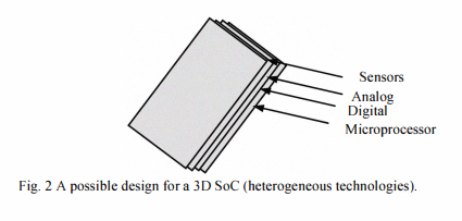
According to the International Technology Roadmap for Semiconductors (ITRS), the traditional scaling will no longer meet the performance and integration requirements of systems-on-chip (SoC) in the long term. Therefore, new I/O and packaging paradigms are needed. Three-dimensional integration is a promising alternative option to traditional 2D planar chips. 3D integration is mainly restricted by the communication infrastructure between different stacked dies of future multi-core SoC and network-on-chip (NoC). Among several 3D integration technologies, the TSV (Through-Silicon-Via) approach is the most promising one and therefore is the focus of the majority of 3D integration R&D activities. However, there are challenges that should be overcome before the production of TSV-based 3D ICs becomes possible, e.g., electrical modeling challenges, thermal and power challenges, technological challenges, design methodology challenges and CAD tool development challenges.